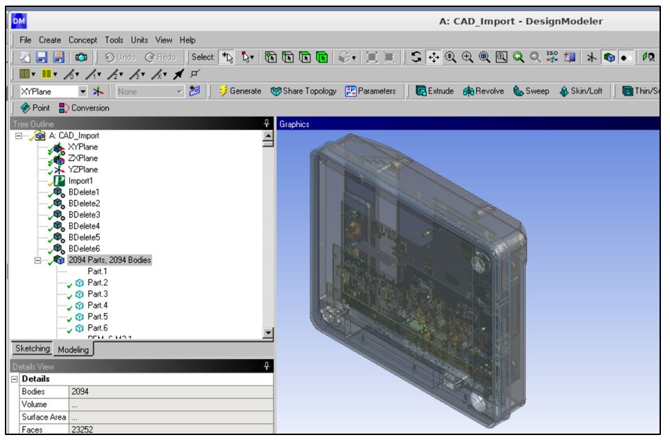
This article describes the workflow for performing electronics cooling analysis on Nimbix platform using detailed PCBs.
To perform an Icepak analysis on Nimbix platform for a system-level analysis that contains detailed PCBs, the following steps can be followed:
GEOMETRY CLEANUP USING DESIGN MODELER
- Start ANSYS platform from the Compute dashboard (use Workbench to import the CAD geometry and prepare it for Icepak CFD software)
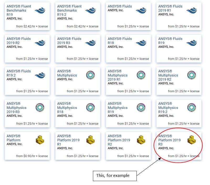
NOTE: If the option is not available in the first page menu, press on “More” at the bottom of the page as shown in the image below:
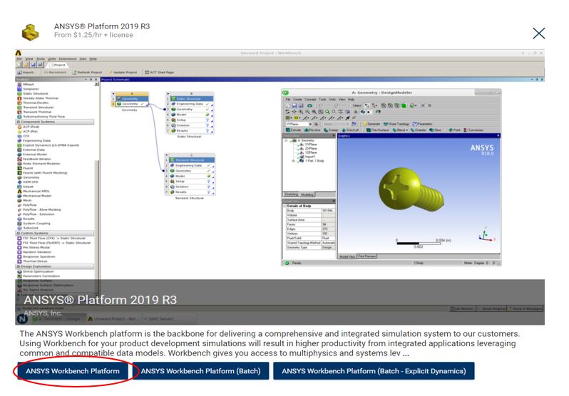
 2. A splash window will open. Select the ANSYS Workbench Platform option as shown below:
3. Cloud set-up screen opens and here you must choose some of your settings by clicking on the Tabs on the top of the window (General, Optional, etc) one tab at a time. Use 1 node for geometry clean-up (lower cost, effective use of licenses, etc). Refer to “ANSYS Platforms Setup Guide” for details.
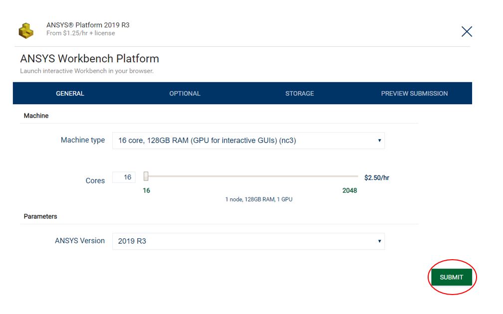
NOTE: When running interactive based applications, you’ll find that selecting an NC9 or any NC* machine types should offer significant visual performance over not selecting an NC machine type. By selecting an NC machine, this places a GPU on your head-node and offers better visual performance. Another thing to keep in mind is that when running interactively you can use a web browser, or in some cases for large models or you might consider using RealVNC.
CAD GEOMETRY IMPORT
4. Import CAD geometry (the CAD file type that can be imported is shown in the Browse option as you right-click on the Geometry and choose “Import Geometry”:
For the current example, a Solidworks Parasolid geometry was imported in the Geometry block.
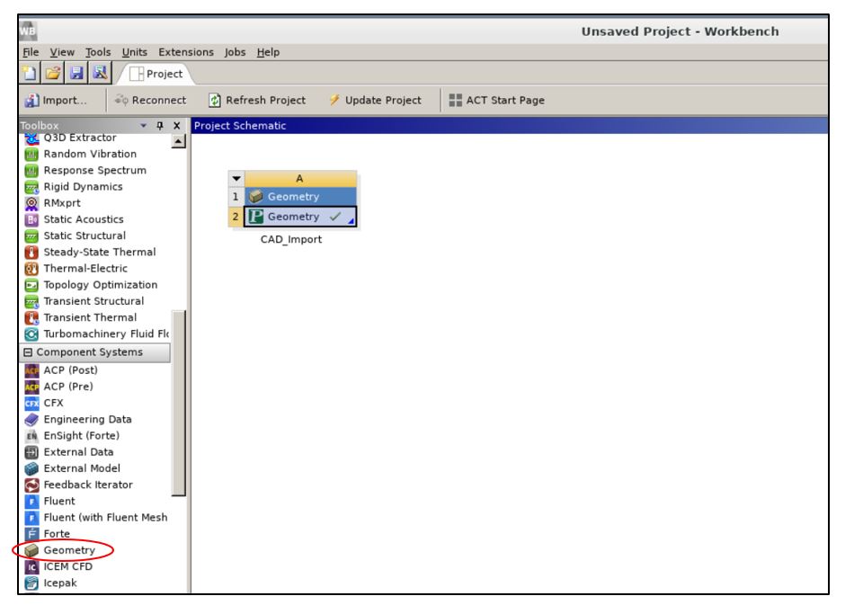
5. Edit the imported CAD geometry file by right-clicking on the “Geometry” box (line 2), shown in the image below as check-marked in green:
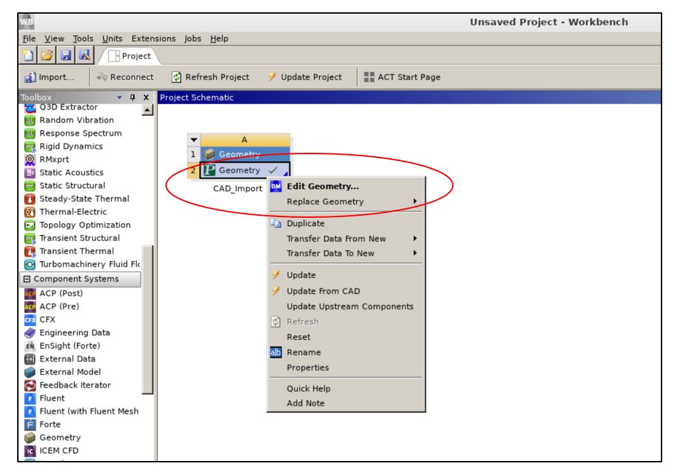
6. Click on “Edit Geometry” from the selection box shown in the previous image. You will now be in the Design Modeler window, where you will need to Import the geometry (you should also select the unit that you want your geometry to be imported into: mm for the current example):
7. Click on the “Generate” button shown in the toolbar (Import has a yellow lightning sign next to it, to show that the task is not yet completed; see the previous image for reference):
NOTE: It is possible that the “Import” icon will remain yellow marked if while importing some of your parts were faulty. You can find the faulty parts by right-clicking on the Import icon and select “Show errors and warnings”. For this example, those faulty parts were ultimately fixed but the Import icon will remain yellow marked.
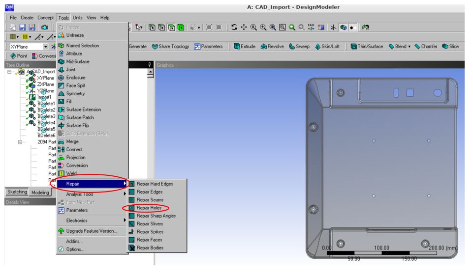
8. Perform clean-up of the CAD geometry to prepare it for simulation (NOTE: most clients will share a detailed CAD model with the analyst, and it is your job to perform simplification and cleaning).
The types of typical cleaning and simplifications are: removing chamfers and fillets, filling in holes that are in the CAD for attachment purposes, remove rounds that are unnecessary, remove small components on a PCB board, such as capacitors, resistors (anything that doesn’t dissipate power).
It is also very important to be sure that parts are in contact if they are supposed to be and they do not interfere with other parts (unless is it supposed to).
For this example, we will show a few of those simplifications:
Under “Tools” on the toolbar, select Repair and Repair holes as shown below:
NOTE: Be sure you select under Find faults now, you select YES.
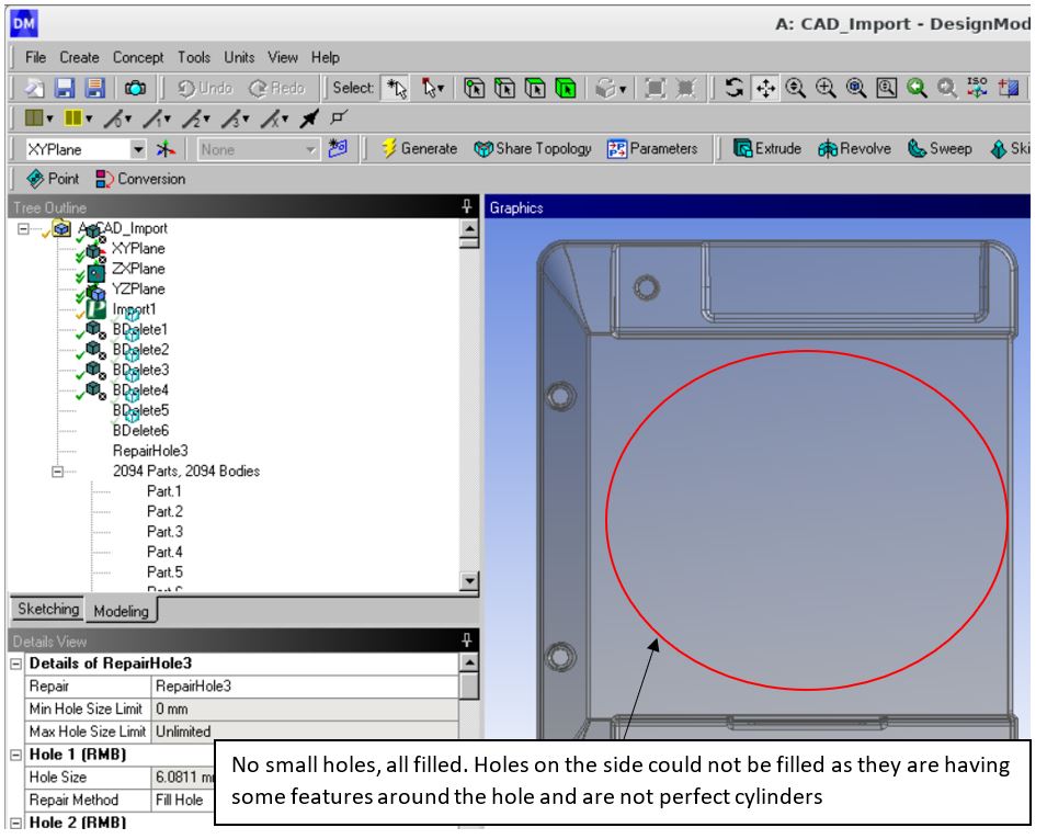
You will have the opportunity to choose to Fill all holes (by default Fill Hole appears) and preserve the holes that are important to be preserved in your model (holes such as vents or big holes used to mount/insert one part into another, you may want to preserve).
NOTE: Not all holes will be filled. The only holes that will be filled without any warnings will be the holes that are perfectly circular and don’t have threads or any other feature around the hole.
For this example, the only holes that were filled/closed were the small holes on the cover, as shown in the image below:
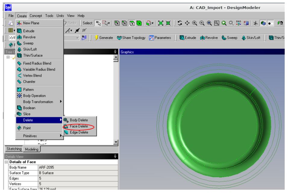
To remove the other holes/features, you may want to zoom in close and use box select (found on the toolbar) and Surface feature select, to select one hole at a time, a shown below:
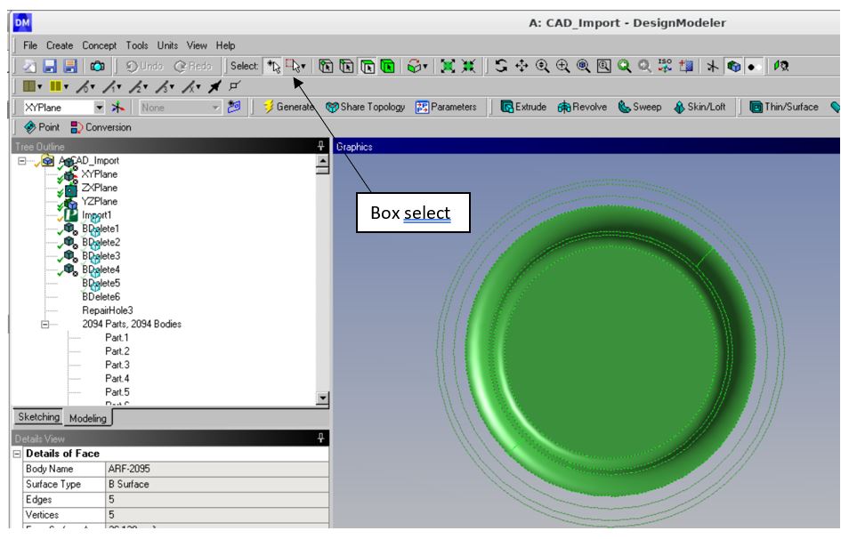
You can now perform the deletion of the selected surface and edges, by going to Create and Delete, and choose Face Delete, as shown in the image below (once selected, click Generate to perform the deletion task):
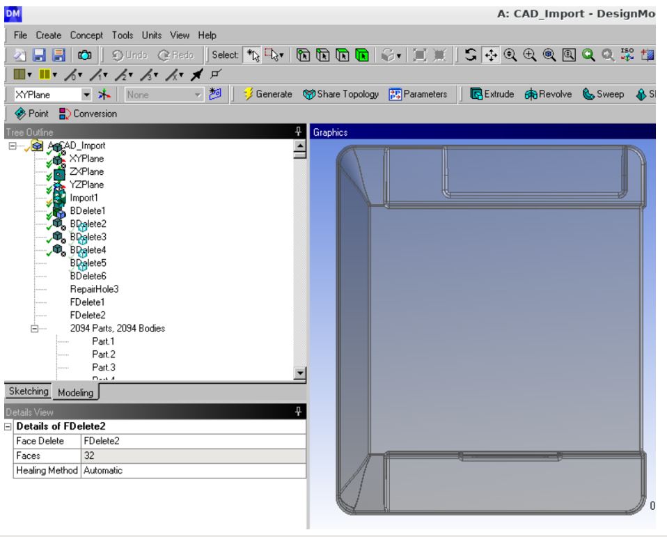
Using this process, you should be able to remove most unnecessary features such as fillets, chamfers, holes, slots, etc (for more information on this topic, review and visit Design Modeler Training material provided by ANSYS):
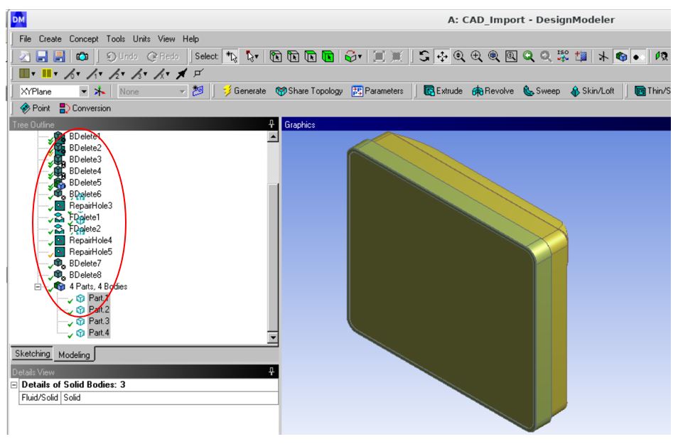
NOTE: As you can see, for this example, the cover is nice and clean and hole-free. There is more room for defeaturing, but just bear in mind that you cannot remove all the features created in CAD using Design Modeler because removing some of the features would lead to some weird and unwanted shapes (Design Modeler is not a CAD tool, it is mainly used to clean up geometries or build simple sketches and geometries).
For the current example, after some cleanup and removal of unnecessary components, we have a clean geometry that is ready to be converted for our CFD ANSYS Icepak analysis:
NOTE: you can see lots of operations in the tree: delete body, repair holes, etc.
9. Perform CAD simplifications to convert the CAD bodies in Icepak objects (keep in mind that Icepak recognizes some of the parts that are Icepak, like primitive parts as Ice-bodies, and automatically will convert those parts. However, if the CAD is not a prism or a cylinder, or polygon that can be recognized by Icepak, you will perform Simplification process using the following steps:
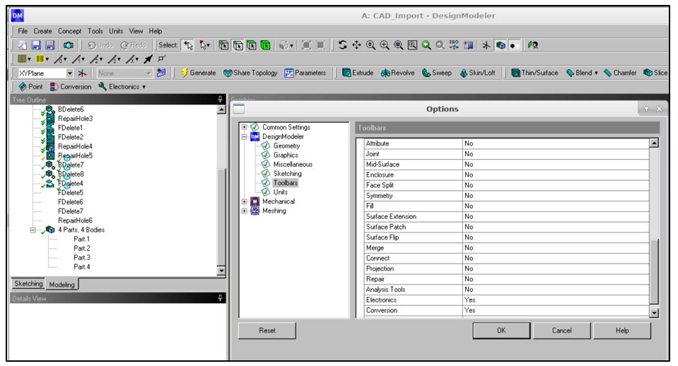
a. Go to Tools button on the toolbar and select Options and under Options (when clicked), under Design Modeler, select Toolbars and next to “Electronics” change the NO (from not being added to your toolbar) to YES.
b. You will now be able to see Electronics button on the Toolbar
10. Click on Electronics on the Toolbar and a window will pop-up:
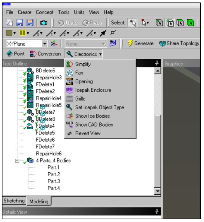
11. If clicked on Show Ice Bodies, in the Graphics window you will be shown the Icepak recognized bodies (aka primitives). If no bodies were recognized as Icepak bodies, nothing will be displayed in the Graphics window.
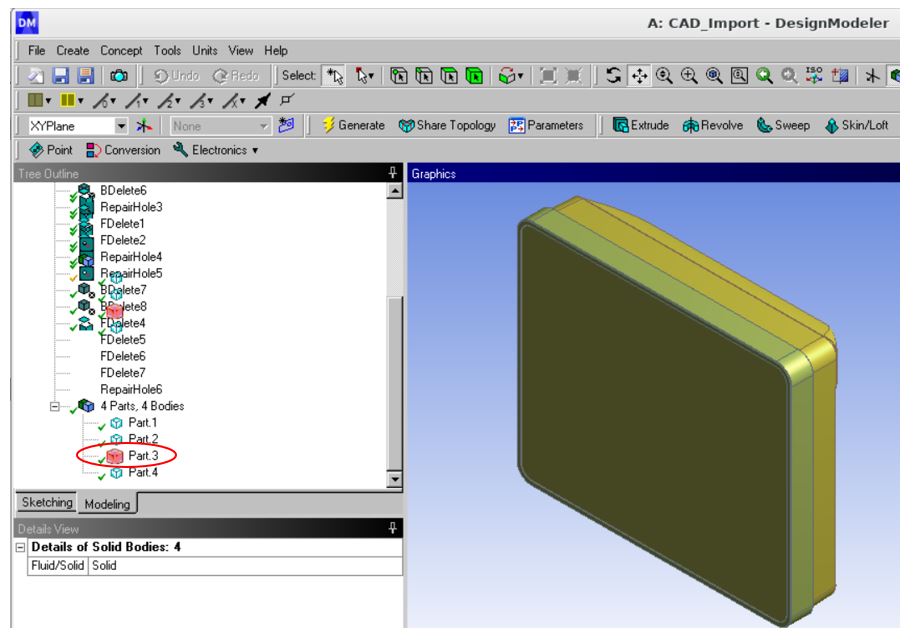
NOTE: For this example, Part 3 was recognized as Icepak primitive body and you can see the red icon next to the part (this shows that Part 3 can be imported now in Icepak)
12. If clicked on Show CAD Bodies, in the Graphics window you will be shown all the CAD bodies that must be converted to Icepak recognized bodies.
13. Once the previous steps are performed, you will need to perform the Simplification process for all the non-recognized Ice bodies, by clicking on Simplify under Electronics (what simplification level should be selected, will depend on your preference; refer to ANSYS Design Modeler CAD simplifications):
14. After completing conversion (Electronics Simplification) of all objects in the tree to Icepak, save your projects and insert an Icepak instance. Link the cleaned geometry to the Standalone Icepak project (drag Geometry over the Model tab and refresh the model)
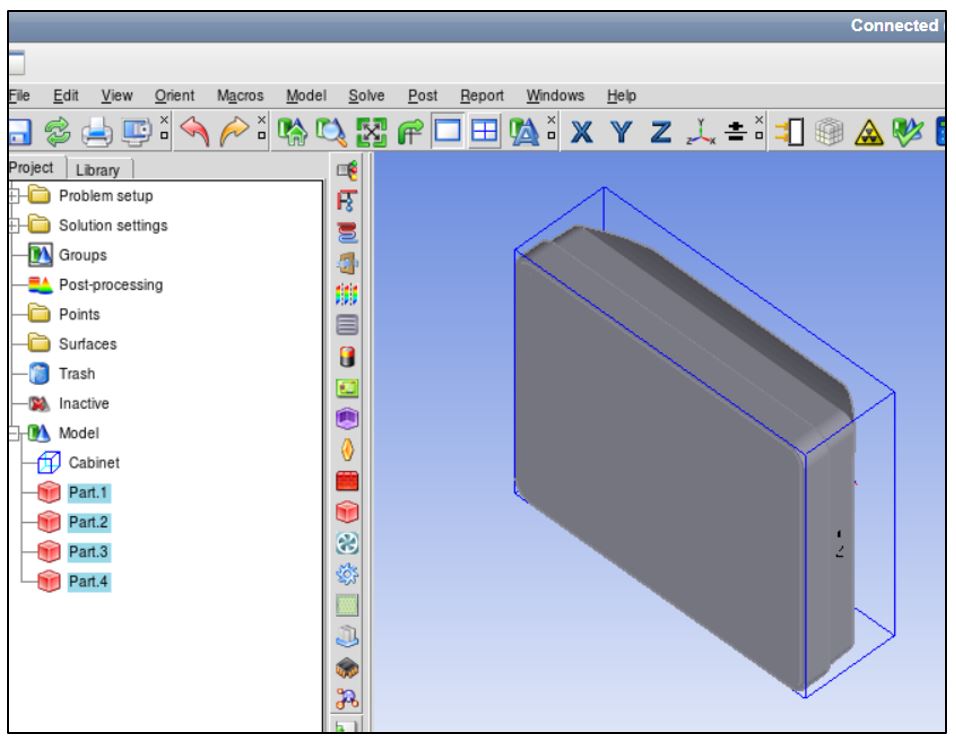
15. In Icepak, under File, pack your project (.tzr extension) and save it to your working folder (/data/YourWorkingFolder). See image below on the Icepak model appearance.
At this point you can save and close your Workbench interface as you will no longer use it.
In the next few steps we will show how to bring in your current Icepak project, a detailed PCB file (detailed PCB here refers to an electrical engineering type of file such as .edb, ODB++, etc). The current example for showing the workflow, will use an ODB++ PCB board type.
Prior to Importing a detailed PCB file, we need to perform some preliminary steps in preparation for importing a detailed PCB using ODB++ file.
PREREQUISITE FOR DETAILED PCB IMPORT IN ICEPAK (NIMBIX)
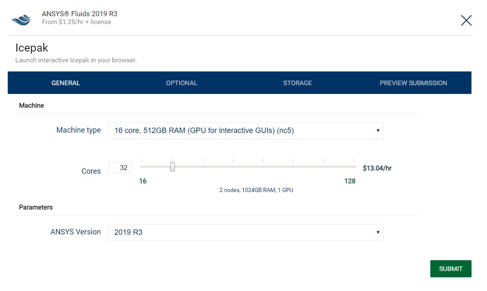
a. From Compute on the NIMBIX interface, choose an ANSYS Fluids release (in this case we will choose ANSYS Fluids 2019 R3) and choose Icepak option from the splash screen:
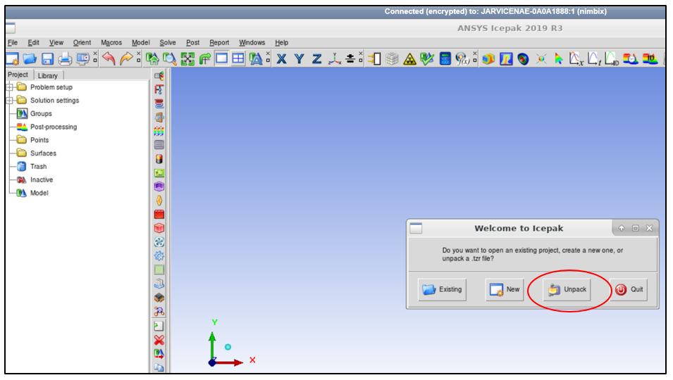
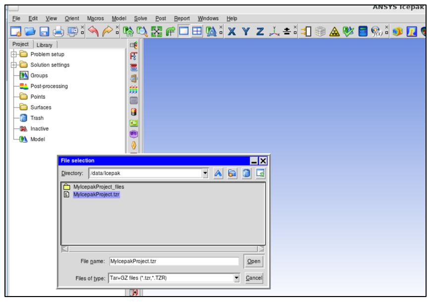
b. Unpack the previously packed Icepak project and save it to your work folder by choosing “Unpack”:
You should look for the folder where you saved the .tzr file:
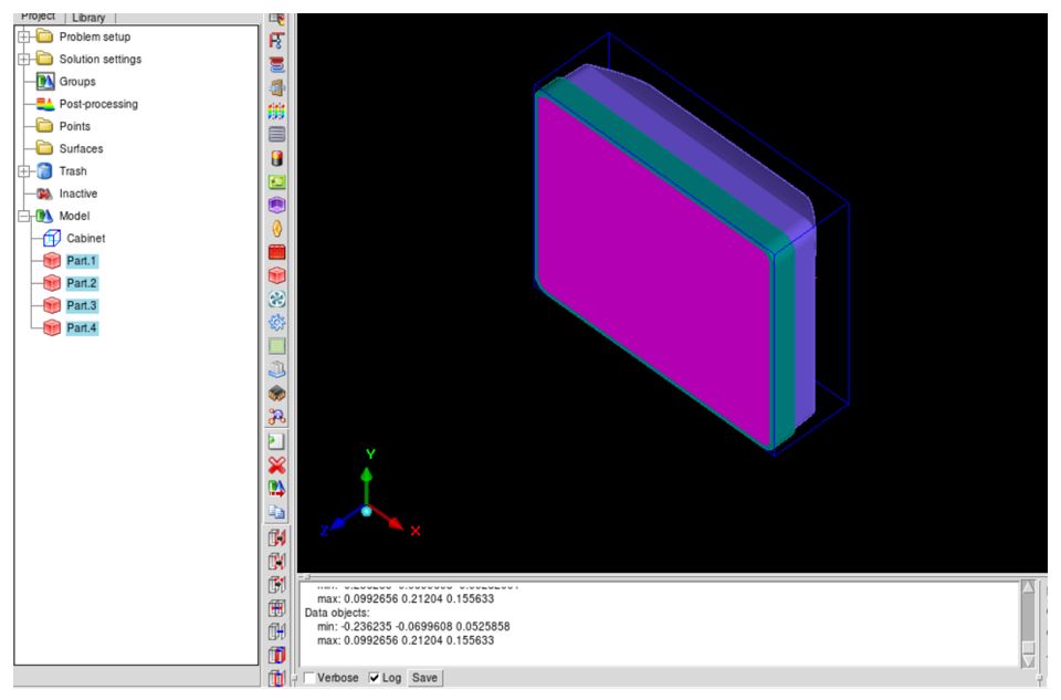
c. After unpacking your project, changing color of the screen for better visibility, and selecting under View the show all solids (selected solids), you are ready to perform other tasks here in Icepak:
At this point, you can save this project and you can even quit the session or put it on hold while we perform the detailed PCB into a separate Icepak standalone project.
DETAILED PCB IMPORT IN ICEPAK
The printed circuit boards (PCBs) can be imported as a detailed PCB design. Having the PCB design file (ODB++ folder) allows Icepak users to bring this board into the system by treating the PCB as a separate project (note that additional information on the PCB board imports is available in the ANSYS Icepak user guide) that can then be packed and imported in the main Icepak project.
Steps for Importing detailed PCB board:
a. Hide the existing objects in the system project (main project) to easily work with the PCB import.
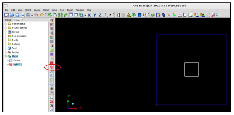
b. Bring in a Prism block from the ANSYS Icepak primitive list (you can also bring in an actual PCB primitive from the list):
c. Open the Prism block by double-clicking on it or right-click and select “Edit”:
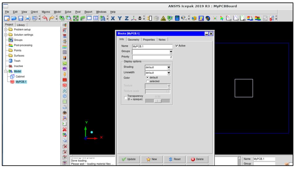
d. Click on the Geometry tab, to be able to Import the ECAD file (for this example it is an ODB++ file):
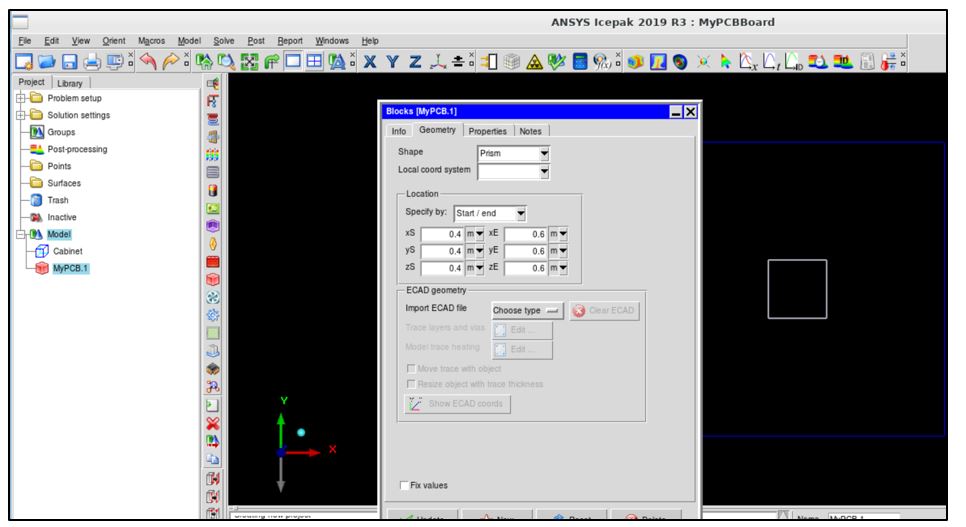
e. In the same “Geometry” display, click next to “Import ECAD file” the “Choose type”
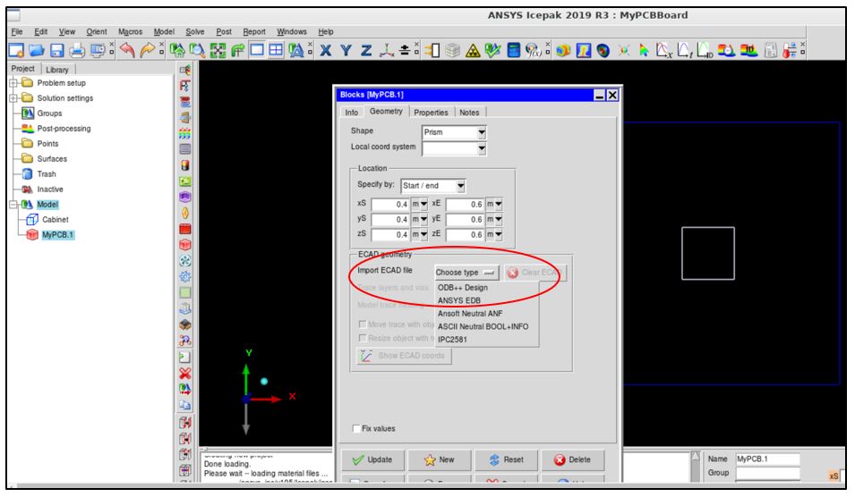
f. You can see the board file types that you can Import ODB++, EDB. Here we will import an ODB++ file (therefore click on ODB++ Design):
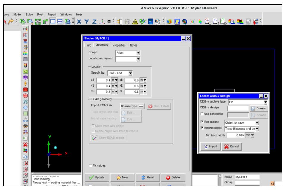
You can see that a small window pops up, named “Locate ODB++ Design”. You can choose the ODB++ to be read from a file (under Browse) or as a Folder (by clicking the caret next to ODB++ archive type). Some of the clients will provide you with a folder instead of a file. In this example, we keep the default type “File”.
g. Browse for your ODB++ file under Browse (be sure you have the ODB++ file loaded in your working data folder that you have your main project saved):
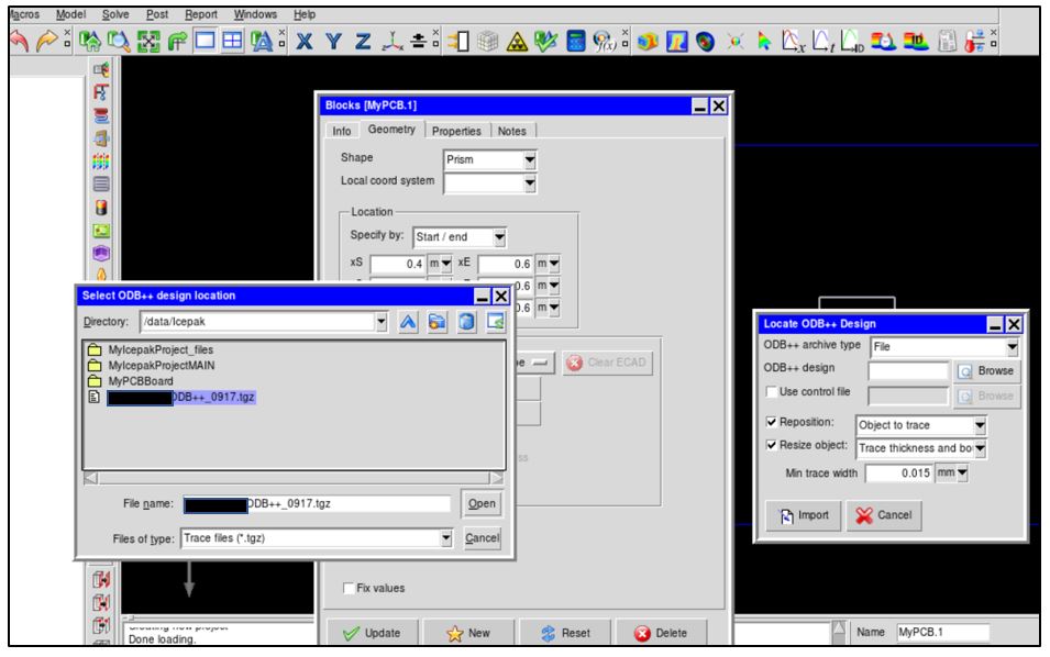
NOTE: For confidentiality purposes, the name of the ODB++ has been grayed out.
h. Click “Open” on the “Select ODB++ design location window” and then click Update on the “Blocks” window. Once those two windows are closed, you can click on “Import” button on the “Locate ODB++ Design” window to import the ODB++ file. It will take few minutes to Import, so wait patiently.
i. The ODB++ file is imported, and you can now see on the screen the details for each layer of the imported board file:
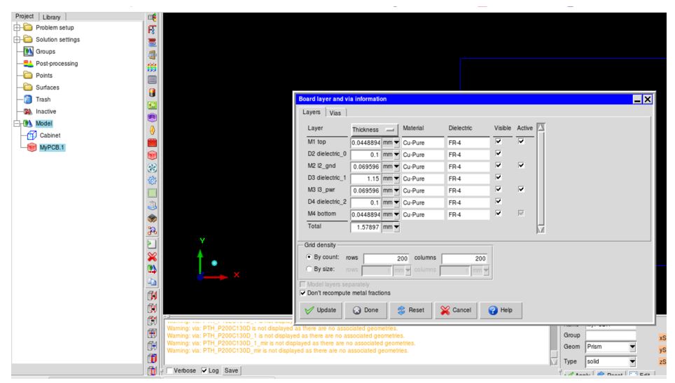
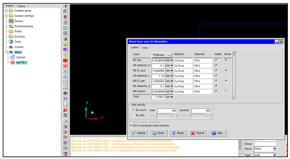
j. Under Grid density you need to choose whether you want the Grid density to be controlled by number of rows and columns or by size. For the current example, the Grid density will be adjusted based on the “By count”. You need to adjust the number of rows and columns (please refer to ANSYS ECAD PCB user guide). Basically, depending on the shape of your board, you want to divide the board in tiny elements called grid. The finer the grid, better you capture the metal fraction in each layer. However, if the number of rows and columns are too high, your metal fraction computation will take much longer and your Icepak PCB file gets bigger. For this example, we chose 800 for rows and 800 for the columns:
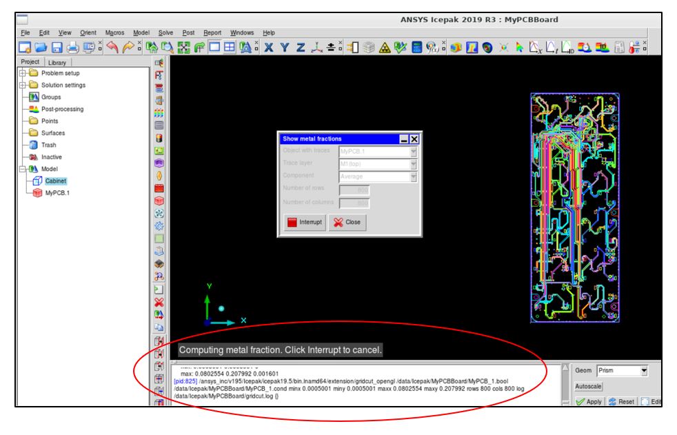
k. Now we are ready to compute the metal fraction, by clicking on Model on the Toolbar and select “Show metal fraction”:
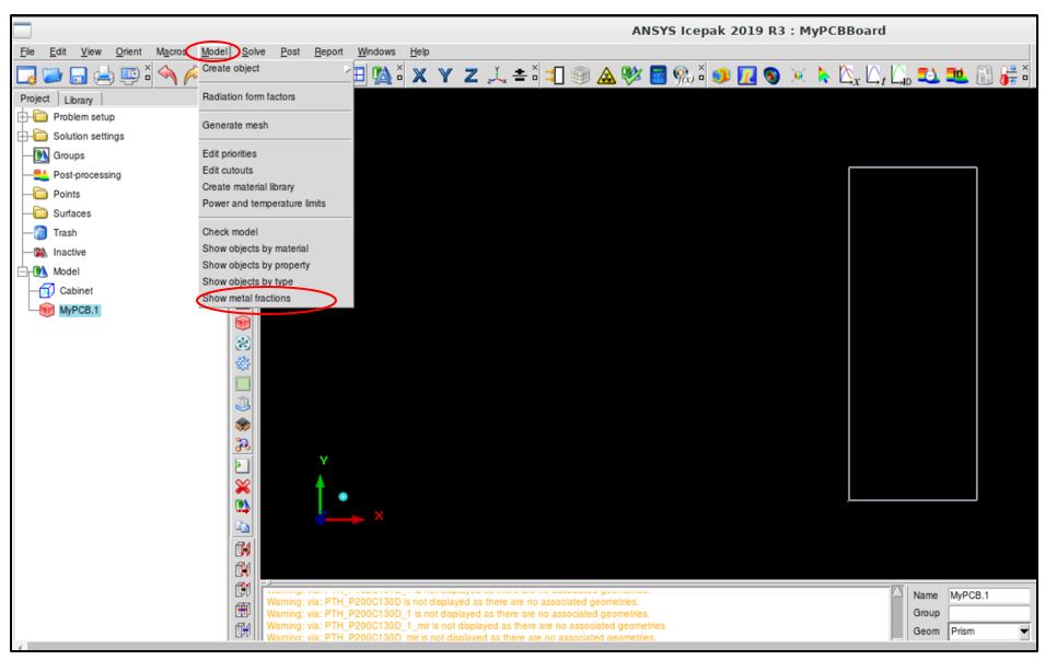
l. After clicking on “Show metal fractions” a small window pops up that looks like the image below:
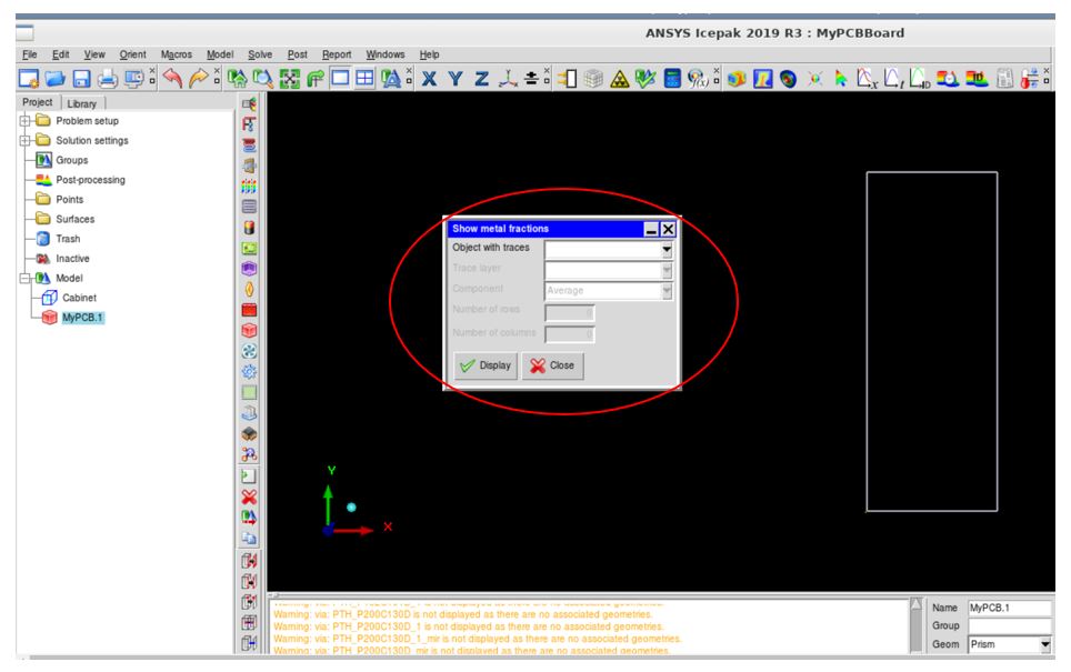
m. Click on the caret next to the “Object with traces” and here you will be able to select the PCB that you wish to see the metal fraction for (in our case our PCB body was called” MyPCB.1”):
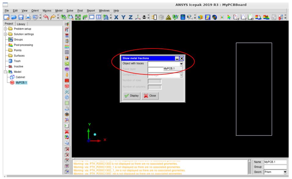
n. By choosing the PCB board, the rest of the rows in the small Table get populated as shown in the image below:
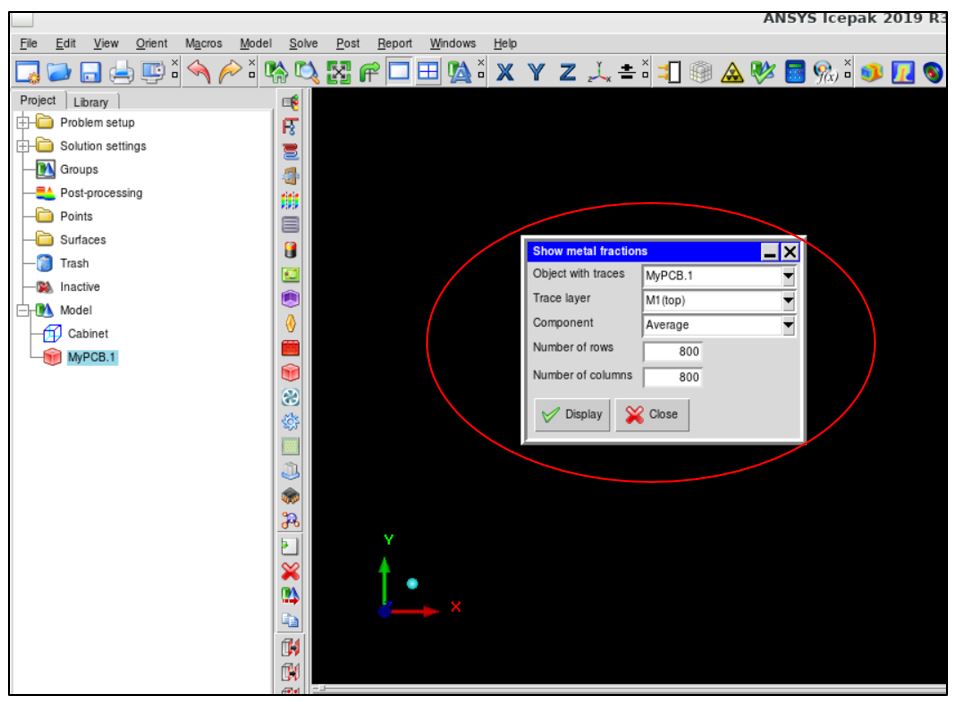
o. Click on” Display” and allow the software to compute the metal fraction (this can take a while if you have many layers in your board, if your board is large and if you choose a high number of rows and columns for generating a fine grid, as mentioned earlier):
Note: Traces will be shown by Default once you imported the ODB++ file. To hide them (so you can better visualize the metal fraction) you can right-click on the MyPCB.1 body in the tree and in the pop-up toggle over Traces and choose “Off”. You can always show them later if you want or need to.
p. You can select a layer at a time by clicking on the caret next to the Trace layer. For this example, we selected layer number 3, which is ground, and you can see in the image below the metal fraction (red means metal fraction and blue means dielectric. Any color in between, such as green, is due to the coarser grid):
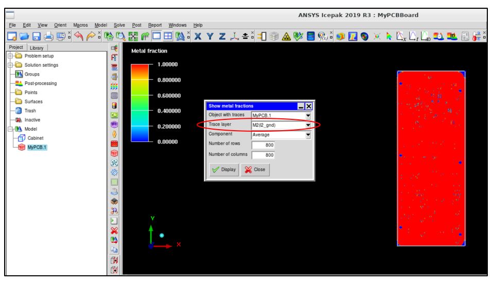
Note: You can even write the “Average metal fraction” which will display the in-plane and through-plane thermal conductivity. To do this, you click on Macro and click on Post-processing and select “Write Average Metal Fraction”. This is useful when you don’t wish to work with the detailed PCB (that has all traces, metal fraction, etc) but rather with an Icepak primitive such as Prism or PCB object and want the computed in-plane and through-plane thermal conductivity.
q. Once a metal fraction of your PCB is computed save your project and close (if desired to add cores to run your model faster).
RUNNING YOUR SYSTEM ICEPAK MODEL ON NIMBIX
Open a standalone Icepak session (follow the same steps as described above) but select 2 nodes (depending on the machine type you chose, for this example that means 32 cores)
NOTE: Do not be tempted to select too many cores. Limit to 2 max 3 nodes to maximize solving efficiency. As the number of nodes increase, the solver will have to spend more time distributing the jobs across multiple computers resulting in time-consuming “slitting/sliding”. The effect is an increase in computation time and possible solution crashing.
Open the saved project and perform FEM setup (default settings, materials, boundary conditions, convergence criteria, analysis solver, mesh settings)
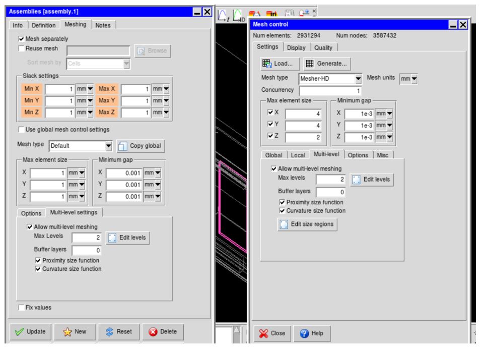
NOTE: For CAD objects in complex assemblies, you can use advanced multilevel meshing for improved convergence at smaller mesh count.
Select “Multilevel Meshing” tab in the assembly/general mesh as needed. Use Level 2, max level 3 as “Max Level” to avoid increasing mesh count too much.
NOTE: Avoid using “0 slack assemblies” with multilevel meshing and check your mesh quality and its skewness before running your job.
NOTE: The multilevel settings in the assembly or general window specify the max levels that can be used on a part in that assembly. Buffer layers ensure a smooth transition between the assembly mesh and the general mesh but, if more refined mesh is desired on a particular part, the “Edit levels button allows the user to enforce a certain level on that part including increasing the level on that part (for example, a level 3 mesh can be applied on a part from an assembly that has a max levels of 2).
SET UP NETWORK PARALLEL OPTION IN NIMBIX
- Open “Solution Setting” in the Icepak tree and select (double-click) “Parallel settings”.
- Choose “Network parallel” (click radio button) as a configuration
- Click on “Browse” button in the “Network parallel options” and navigate (use the /\ - UP button) to /etc/JARVICE folder.
- Double-click the file named “cores” to set up your cores
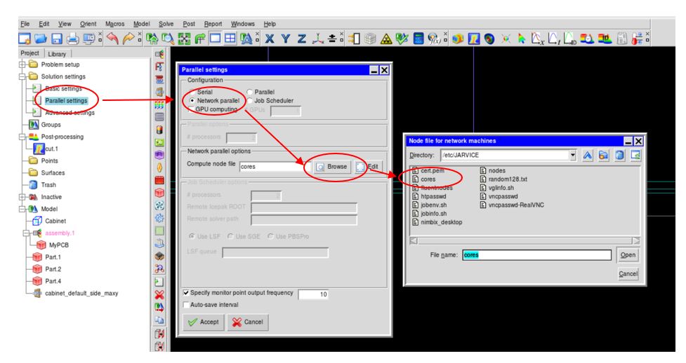
Click “Open” and accept the network parallel settings
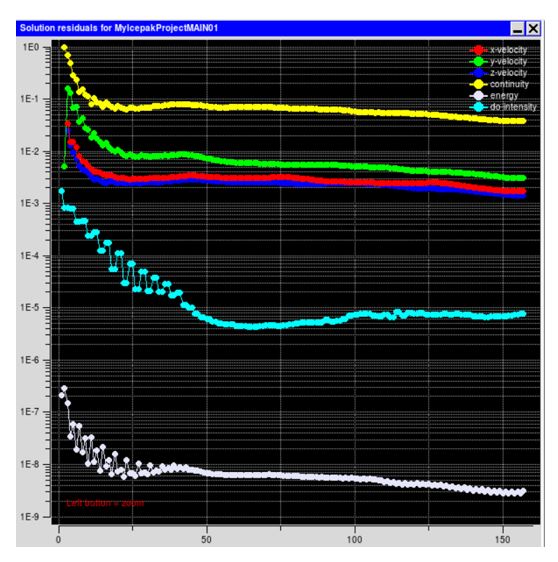
Run your solution (examine your residuals convergence in the graphics window):
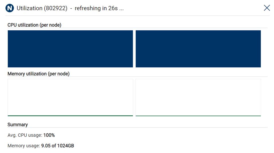
Check “Detailed Job Metrics” to see the utilization of your nodes during Solve:
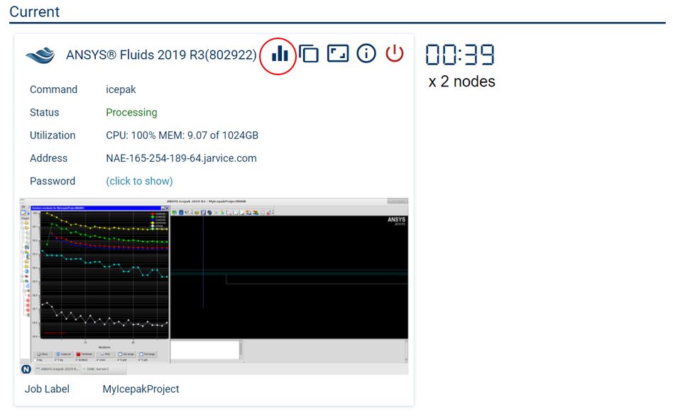
Node utilization will appear as a pop-up window. Utilization is usually smaller at the beginning of the simulation since some of the tasks may not be distributed across multiple nodes.
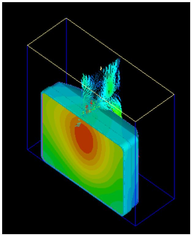
After the model finished running, post-process as desired (temperature profiles, flowlines, velocity vectors, pressure drops, etc):